PRODUCTS
PRODUCTS
PRODUCTS
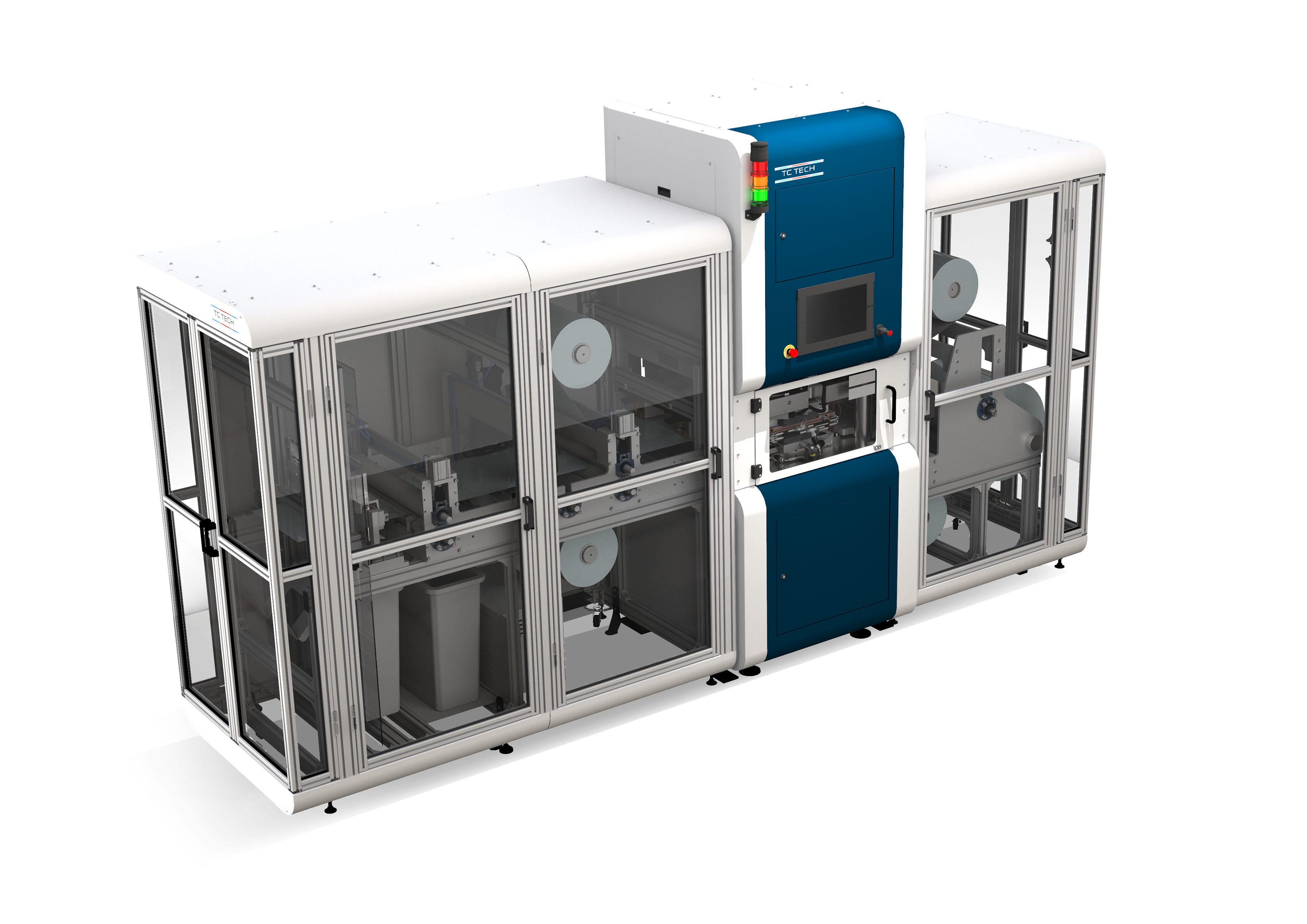
EMBOSSING MACHINE TCP 170
The TCP 170 is the ideal system to produce advanced double/single sided patterns in polymerfilms. With a submicron resolution and near perfect replication the next generation of patterns can be produced efficiently.
- Max quality area: 370 x 235 mm 5”-17”, screens with various aspect ratios and multi-cavity.
- Pattern: advanced double-sided patterns with alignment, optional taper/wedge
- Thickness: down to 0.10 mm
- Cycle time: down to 30 seconds depending on application and on thickness, pattern, and material
- Substrate: any thermal polymer, but most common are PC or PMMA.
- Application dimension: Up to 17”
- Certification: CE

Automatic input and output of plastic film. A roll of film substrate, with or without protective film, is placed in the system. Any protective film is automatically removed on both sides and the substrate film is deionized and vacuum cleaned. Film width of up to 450 mm is adapted for a 370 mm wide quality area.
TC TECH technology is based on a unique induction heating process, where only the
stamper is heated. The press and tool solution include several patented innovations that deliver
full pressure uniformity to achieve near perfect replication.
By leveraging years of experience in materials research, the TCP 170 provides the necessary freedom through a
simplified design for volume production. TCP 170 will offer excellent precision and reproducibility for a wide spectrum
of applications to industry and academia.
THE TOOL
THE TOOL

Suitable for any polymer substrate up to 370mm x 235mm.
Our tool makes it possible to manufacture optical films and diffusers in the same production equipment to the three most common laptop screen sizes: 13, 15 and 17 inches.
Also smaller plastic parts, such as for microfluidics, also fit well in the tool. Multiple cavitities can then be utilized to enhance productivity.
Unique tools can be specially designed based on the customer’s specific requirements and wishes.

MASTERS AND STAMPERS
MASTERS AND STAMPERS
With near perfect replication achievable down to nano level the precision and quality of the stamper becomes crucial. Stampers are mainly made in electroformed nickel or stainless steel depending on the type of pattern which is requested. A simple dot pattern can be made with laser or etching. Advanced micro lens arrays need a more complex manufacturing method including a lithography process (2D or 3D) to make a master for the production of the stamper in electroformed nickel.
To achieve the best result, the stamper should have a thickness between 0,6 mm to 1,0 mm with a good thickness uniformity. Maximum patterning area (quality area) is 370×235 mm. Stampers can normally be used for several hundred thousand cycles with adequate maintenance. A master for the electroforming process can be used to produce several identical stampers. For more information and discussion about what’s the best solution for your project, contact TC TECH direct.
| Stamper size: 424x285mm Quality area: 370x235mm |
Polished stainless steel Laser/Etching Steel stamper |
Electroplated steel Diamond milling Steel /nIckel stamper |
Elctroplated steel (2) used as a master Electroformed stamper |
Lithography master 3D or 2D Electroformed stamper |
|---|---|---|---|---|
| Mirror | x | x | x | x |
| Laser dot / Etched | x | x | x | |
| Wedge | x | x | ||
| V-cut | x | x | ||
| Lenticular | x | x |

